College of Engineering News Room
New method to improve durability of nano-electronic components to help further semiconductor manufacturing and resilience
USF Mechanical Engineering assistant professor Michael Cai Wang’s group recently developed a novel approach to effectively mitigate electromigration, a phenomenon that has long posed challenges for the semiconductor and integrated circuits industry.
USF Mechanical Engineering assistant professor Michael Cai Wang and his research team recently developed a novel approach to mitigating electromigration in nanoscale electronic interconnects that are ubiquitous in state-of-the-art integrated circuits. This was achieved by coating copper metal interconnects with hexagonal boron nitride (hBN), an atomically-thin insulating two-dimensional (2D) material that shares a similar structure as the “wonder material” graphene.
Electromigration is the phenomenon in which an electrical current passing through a conductor causes the atomic-scale erosion of the material, eventually resulting in device failure. Conventional semiconductor technology addresses this challenge by using a barrier or liner material, but this takes up precious space on the wafer that could otherwise be used to pack in more transistors. Wang’s approach accomplishes this same goal, but with the thinnest possible materials in the world, two-dimensional (2D) materials.
Ångström-thin hexagonal boron nitride (hBN) is a highly promising barrier/liner dielectric material for passivating electrical interconnects in ultra-scaled integrated circuits (ICs). Yunjo Jeong (USF graduate student in Mechanical Engineering) and co-workers developed a novel approach to mitigating electromigration in nanoscale copper interconnects. Significant improvements in the breakdown current density and operating lifetime are observed in hBN-passivated copper interconnects, paving the way for further single-nanometer node scaling of semiconductor and ICs manufacturing.
“This work introduces new opportunities for research into the interfacial interactions between metals and ångström-scale 2D materials. Improving electronic and semiconductor device performance is just one result of this research. The findings from this study opens up new possibilities that can help advance future manufacturing of semiconductors and integrated circuits,” Wang said. “Our novel encapsulation strategy using single-layer hBN as the barrier material enables further scaling of device density and the progression of Moore’s Law.” For reference, a nanometer is 1/60,000 of the thickness of human hair, and an ångström is one-tenth of a nanometer. Manipulating 2D materials of such thinness requires extreme precision and meticulous handling.
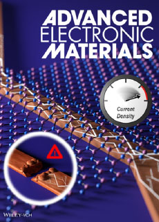
In their recent study published in the journal Advanced Electronic Materials, copper interconnects passivated with a monolayer hBN via a back-end-of-line (BEOL) compatible approach exhibited more than 2500% longer device lifetime and more than 20% higher current density than otherwise identical control devices. This improvement, coupled with the ångström-thinness of hBN compared to conventional barrier/liner materials, allows for further densification of integrated circuits. These findings will help advance device efficiency and decrease energy consumption.
“With the growing demand for electric vehicles and autonomous driving, the demand for more efficient computing has grown exponentially. The promise of higher integrated circuits density and efficiency will enable development of better ASICs (application-specific integrated circuits) tailored to these emerging clean energy needs.” explained Yunjo Jeong, an alumnus from Wang’s group and first author of the study.
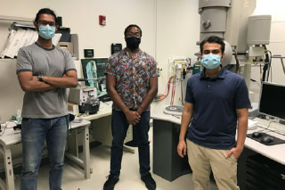
Researchers from the Nanomechanics, Nanomaterials, NanoManufacturing Laboratory (NM3L) who contributed to this work (from left): Utkarsh Misra (sophomore in Electrical Engineering), Ossie Douglas (PhD student in Mechanical Engineering), and MD Rubayat-E Tanjil (PhD candidate in Mechanical Engineering).
An average modern car has hundreds of microelectronic components, and the significance of these tiny but critical components has been especially highlighted through the recent global chip shortage. Making the design and manufacturing of these integrated circuits more efficient will be key to mitigating possible future disruptions to the supply chain. Wang and his students are now investigating ways to speed up their process to the fab scale.
“Our findings are not limited only to electrical interconnects in semiconductor research. The fact that we were able to achieve such a drastic interconnect device improvement implies that 2D materials can also be applied to a variety of other scenarios.” Wang added.
This project was in collaboration with researchers from the National Institute for Materials Science (NIMS) of Japan and was supported in part by the University of South Florida (USF) New Researcher Grant (NRG), USF Nexus Initiative (UNI), the ORAU Ralph E. Powe Junior Faculty Enhancement Award, and the National Science Foundation under Grant No. 1944638. Support was also provided in part by the National GEM Consortium Fellowship, Alfred P. Sloan Minority Graduate Scholarship Program, and USF University Graduate Fellowship. Extensive experimental work was completed at the USF Nanotechnology Research and Education Center (NREC).