College of Engineering News Room
Two EE Faculty Receive Patent and NSF Grant for Wearable Technology
The electrical engineering professors are advancing wearable electronics.
Wearable electronics are becoming increasingly common, with clothing wired to connect to a range of devices like headphones nestled inside a hat. Expanding on previous work in this area that resulted in a patent approved this year (A. Takshi, SM Rosa-Ortiz, Patent No. 11,214,884), Department of Electrical Engineering Associate Professor Arash Takshi and USF Research & Innovation Interim Vice President and Professor Sylvia Thomas are using a novel electrochemical method to print copper directly on fabric.
With a $369,574 grant from the National Science Foundation, the project is taking wearable electronics to a whole other level.
The type of technology that can be embedded into fabric is limited only by the imagination, and Takshi sees his invention primarily beneficial in several sectors — health, military and personal performance monitors. Smart suits can be designed for military personnel and astronauts with distributed sensors interconnected using this new technology. Smart suits can also be designed for monitoring a patient’s health status and the physical activities of athletes.
“The current technology for wearable electronics is mainly based on printing conductive inks consisting of nanoparticles of metals and/or carbon,” Takshi said. “The process relies on the physical connections of nanoparticles after drying the pattern. However, the high electric resistance from a conductive path made of conductive nanoparticles limits the applications to simple wearable electronic designs. These aren’t suitable for sensitive measurements and high electric current applications.”
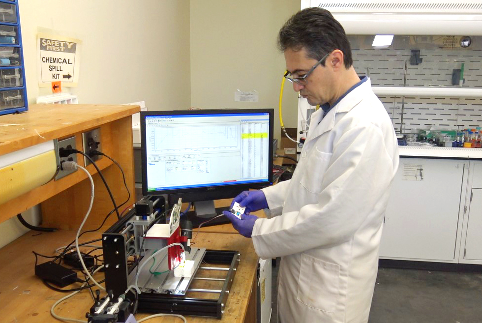
Associate Professor Arash Takshi in the Bio-Organics Electronics Lab.
More importantly, soldering electronic components to fabrics is a serious challenge, as the conventional soldering method using a soldering iron can damage the fabrics, and the conductive pastes are not durable for wearable electronics.
The new fabrication method is a two-step additive manufacturing process. First, a conductive template is applied to fabrics using laser printing, which carbonizes them. Then, electroplate copper produces a continuous copper pattern that forms the circuit layout.
By designing a nozzle mounted on a 3-D printer platform, localized electroplating is now feasible. With this method, copper can be grown at the junctions between the electronic components’ terminals and the circuit printed layout to solder them at room temperature.
This novel process resembles 3D printing if one could 3D print a material at the nanoscale, and its development has been supported through the use of equipment at the Advanced Membrane and Materials Bio and Integration Research Laboratory, (AMBIR) managed by Thomas.
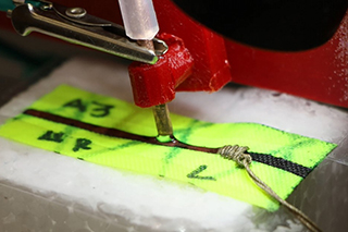
Printing directly on fabric, taking wearable technology to a higher level.
Thomas, the project’s co-principal investigator, said that the resulting invention has the potential to change the entire production pipeline of wearable electronics.
“This technology stands to further advance the way we envision wearable electronics, textile electronics, and flexible electronics as we know them today – from lab to innovation to product,” she said.
Although copper electroplating has been used for years, conventional electroplating uses low voltages and high currents that deposits copper at a rate as slow as a few hundred nanometers per second. With such a rate, it takes hours if not days to print a circuit layout on a piece of clothing.
In the devised method, invented by Takshi and his former Ph.D. student, Sabrina Rosa-Ortiz, a few volts are applied for growing copper. The relatively larger voltage, still in the range of 2-3 V, results in water electrolysis at the same time that copper grows.
This method — called hydrogen evolution assisted (HEA) electroplating — pushes the limitations in the copper growth, achieving rates three orders of magnitude higher than conventional electroplating.
More importantly, the concurrent process of electroplating and water electrolysis results in a growing fern-shape copper structure that penetrates into the fibers of the fabrics enhancing the mechanical stability of the printed structure.
The ability to miniaturize the device circuitry making it adherable to fabrics and other surfaces could change forever the manufacturing of wearable technology.
Watch this video to learn more about the hydrogen electroplating process.